Common Design

Design Constraints Table

Figure 1: Illustrated Proposed Amplifier Design
The goal of this project is to design a fully-differential high-speed high-precision amplifier with the following design specifications shown in the table to the right.
Keeping this in mind, the project also specifics two different designs that satisfy different objectives.
Design 1: Minimize Large-Signal Settling Time to 0.5% accuracy, Power Budget of 20mW
Design 2: Minimize power dissipation, 0.5% large-signal settling time of 40ns
As a first round pass, our team decided to start with a 5 transistor operational transconductance amplifier and build off of whatever deficits exist in the design.
In order to properly bias the amplifier, it’s necessary to know the relevant values of the figures of merit that we must design to. In a closed-loop negative feedback system we know that VoutVin = H(s)1+G(s)H(s), where H(s) is the open loop transfer function and G(s) is feedback transfer function . Referencing the illustrated representation of a finalized differential amplifier design in figure 1, we can draw out symbolic expressions for open loop gain (A0) and closed-loop gain, and come out with the following expression:

With a gain error of less than 1%, we know that [ (1+Z2/Z1)(1/A0) ] should not exceed 0.01, and with the closed loop gain requirement, we know that (Z2 / Z1) = 8, meaning that A0 is greater than or equal to 900.
Design Exploration
5 Transistor Operational Transconductance Amplifier 1st Stage Design
The absolute maximum power dissipation of both designs is 20mW, with VDD = 1.8V that leaves ~11mA of supply current total for the amplifier design. As a first-pass conservative design, we go for a current mirror reference of 500uA for NMOS current mirror biasing, and 500uA for PMOS current mirror biasing; leaving 5mA maximum for each branch of the differential pair. Additionally, a differential swing requirement of 1.8V implies a single-ended swing requirement of 0.9V. Given the single-ended swing requirement, we are left with 0.9V that must be distributed among the transistors in the current path; leading us to aim for a drain-source voltage of 300mV per transistor (300mV for current source load, amplifying transistor, and tail current source)

Figure 2: Transistor Sizing Method
With a requirement for drain-source voltage, the following circuits (Figure 2) were built in cadence in order to determine the required widths for the transistors to support the required current (we will employ a conservative 1mA for differential legs and 2mA for the tail current source in this design).
In order to size the transistors according to the method shown in figure 2, we start with a desired current (5mA for differential leg transistors and 10mA for the tail transistor). The resistor value is chosen such that R*Ibias=Vth, guaranteeing saturation because the gate voltage will be one threshold above the drain. Transistor sizing is done by increasing the width such that the drain-source voltage is equivalent to our desired value (300mV per transistor in this design example).
The design procedure described above yields the following result (Figure 3):

It’s clear to see that the 5-transistor OTA that we designed is nowhere near our desired open loop gain of 900 that we need in order to meet our gain error criteria. In this case it would be beneficial to switch the topology to that of a telescopic cascode, to improve the differential gain at the cost of differential output swing.
Design Exploration
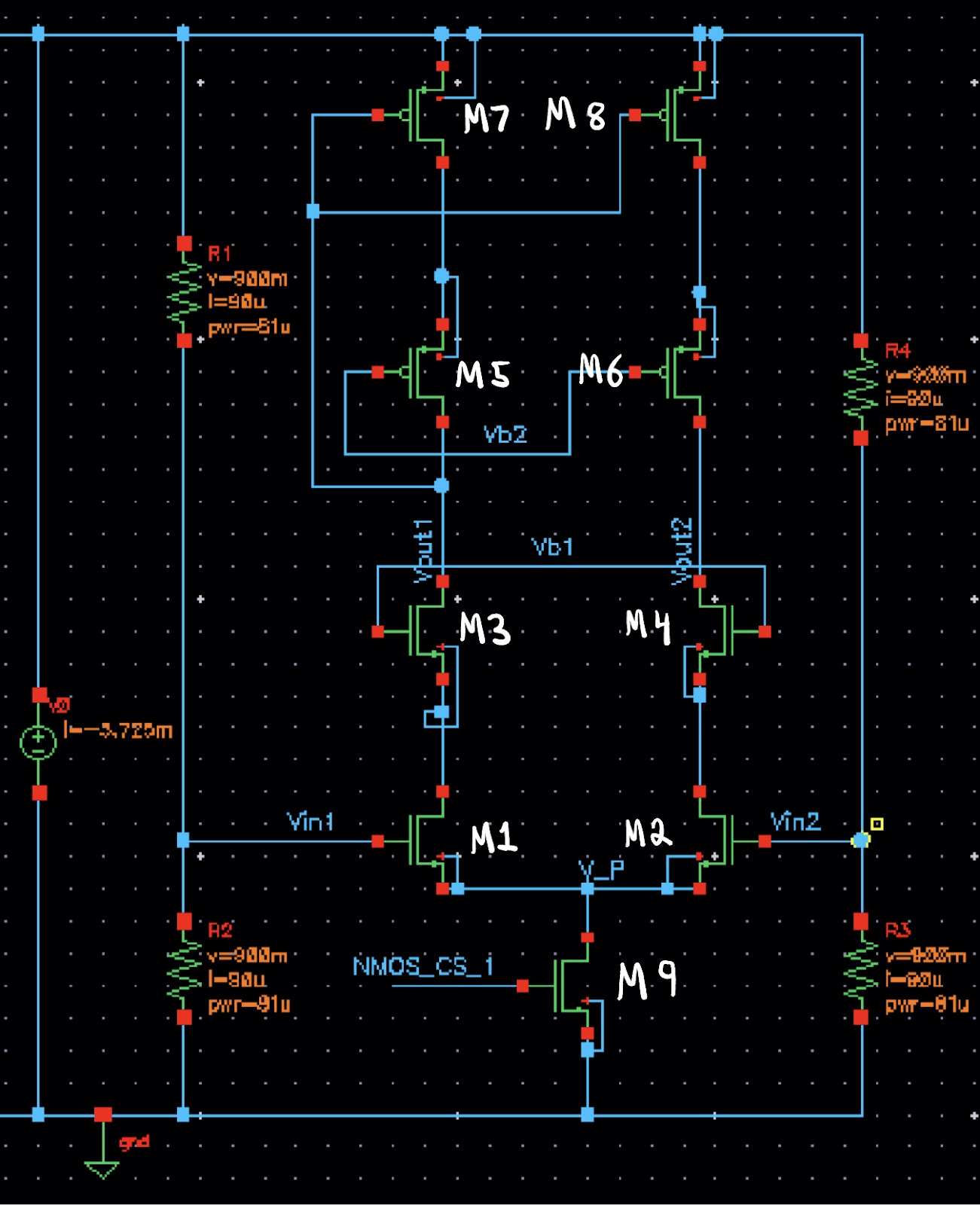
Figure 4: Telescopic Cascode 1st Stage Differential Amplifier
In order to increase the amplifier gain from the previously designed 5 Transistor OTA, the approach of using a telescopic cascode was explored. The Telescopic Cascode has a gain defined by: |Av| = gm_n(gm_n*ro_n2 || gm_p*ro_p2) which is considerably higher that the previous gain of |Av| = gm_n(ro_n || ro_p) realized by the 5 Transistor OTA. In addition to the higher intrinsic gain of the amplifier topology, additional gain can also be realized by dropping the bias currents as well. The major drawback of the telescopic cascode is its lack of output swing so we based this design on the assumption that we will require a second stage to meet our design requirements.
With an open-loop gain requirement of 900, we will aim for 100 in the first stage (telescopic cascode) and 9 in the second stage. A gain of 9 in the second stage allows us to restrain our single-ended swing in the first stage to 100mV. The sum of 5 drain-source voltages in a single leg of the first stage must now add up to 1.8V – 100mV = 1.7V. In this new topology we distribute the headroom among the transistors in the following manner: 400mV per PMOS and 300mV per NMOS. In this design case we also design for a conservative 2mA tail current, meaning a bias current of 1mA per leg.
In order to properly bias this topology, M7/M8 were biased with a standard PMOS current mirror, M5/M6 were biased with a PMOS variation of a low-voltage cascode mirror, M3/M4 were biased with a NMOS variation of a low-voltage cascode mirror, and M9 was biased with a standard NMOS current mirror
Upon simulating the results of the telescopic cascode stage, we began to notice signs of instability. In the DC operating point of the Telescopic Cascode Design, we can observe that due to mismatches, the bias currents in each differential leg are not exactly equal to Iss/2, which forces the output common-mode level to rail up to VDD or down to ground. In order to combat this phenomenon, we look to employ a form of common-mode feedback for compensation. The issue of common mode feedback stems from differences in the currents from the PMOS and NMOS cascode sections of each telescopic cascode branch. Acting as ideal sources, the cascode sections try to impose a certain current through the branch, but process variations and temperature changes cause them to fight against each other, saturating the output common mode level high or low. To fix this issue, we employ common-mode feedback in the described manner (Figure 5):

Figure 5: Telescopic Cascode with CMFB
The common-mode feedback in this topology (Figure 5) works by having M9 and M10 sense the output common mode level through their gate terminals. Increases/decreases that would alter the output common-mode level are negated by increases/decreases in the tail current. This feedback topology allows common-mode sensing without loading the high impedances at the output nodes that allow for a high gain.

Figure 6 shows that our initial design was successful in realizing a large open loop gain; and with a desired two-stage open loop gain of 900, we decrease our expectations of the 2nd stage gain to only ~2.2 which is easily achieved with a 5 transistor OTA as shown in figure 3. The final device sizes for our designs can be found in the table below.
*C1/C2 DC Blocking Caps , **C9/C10 and **C5/C6 are 10% parasitic caps
| Device | Initial TC design | Settling Optimized | Power Optimized |
| M1/2 | 120um/0.3um | 120um/0.3um | 120um/0.3um |
| M3/M4 | 120um/0.3um | 120um/0.3um | 120um/0.3um |
| M5/M6 | 180um/0.3um | 180um/0.3um | 180um/0.3um |
| M6/M7 | 180um/0.3um | 180um/0.3um | 180um/0.3um |
| M8/M9 | 180um/0.3um | 180um/0.3um | 180um/0.3um |
| M9/10 | 120um/0.3um | 120um/0.3um | 120um/0.3um |
| M11/M12 | N/A | 300um/0.3um | 90um/0.3um |
| M13/M14 | N/A | 50um/0.3um | 15um/0.3um |
| M15 | N/A | 3um/0.3um | 3um/0.3um |
| M16 | N/A | 1um/0.3um | 1um/0.3um |
| M17 | N/A | 1um/0.3um | 1um/0.3um |
| M18 | N/A | 1um/0.3um | 1um/0.3um |
| M19 | N/A | 1um/0.3um | 1um/0.3um |
| M20 | N/A | 1um/0.3um | 1um/0.3um |
| M21 | N/A | 1um/0.3um | 1um/0.3um |
| M22 | N/A | 8um/0.3um | 8um/0.3um |
| M23 | N/A | 1um/0.3um | 1um/0.3um |
| M24 | N/A | 1um/0.3um | 1um/0.3um |
| M25 | N/A | 1um/0.3um | 1um/0.3um |
| M26 | N/A | 1um/0.3um | 1um/0.3um |
| I_ref | N/A | 90uA | 50 uA |
| C1/C2* | N/A | 1 F | 1 F |
| C3/C4 | N/A | 5 pF | 2.4 pF |
| C5/C6** | N/A | 0.5 pF | 0.24 pF |
| C7/C8 | N/A | 625 fF | 300 fF |
| C9/C10** | N/A | 62.5 fF | 30 fF |
| C11/C12 (Load) | N/A | 2 pF | 2 pF |
| C13/C14 (M-Comp) | N/A | 1 pF | 2 pF |
| R1/R2 | N/A | 400 KOhms | 50M |
| R3/R4 | N/A | 600 KOhms | 60M |
| R5/R6 (M-Comp) | N/A | 600 Ohms | 250 Ohm |
| R7/R8 | N/A | 1 KOhms | 1 KOhms |
Currents
| Single Branch Bias Current | Settling Optimized | Power Optimized |
| Stage 1 | 1.536 mA | 802 uA |
| Stage 2 | 679.6 uA | 424 uA |
| Total Amplifier | 4.43 mA | 2.452 mA |
| Total (including biases) | 4.859 mA | 2.85 mA |
| Total Power | 8.74 mW | 5.13 mW |
Design Exploration
Settling Time Optimized Closed Loop Design

Figure 7: Two Stage Amplifier Design for Settling Time Optimization
With the first stage design finished, efforts switched to the second amplifier stage as well as the closed loop design in order to reach the other design requirements.
The outcome of the first stage telescopic cascode design was a gain of roughly ~400, meaning that the 2nd stage design can be a 5 transistor OTA with a gain of roughly ~2.2.
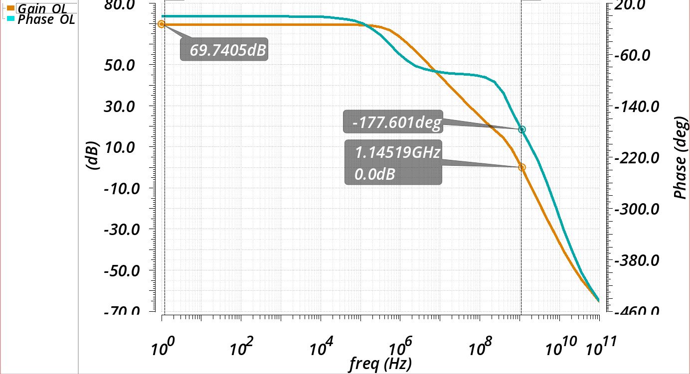
Referencing Figure 8, by the end of the design process, we were left with an open loop DC gain of 69.74dB (roughly a gain magnitude of 3000) which is way higher than the initial minimum constraint of 900 open-loop gain that was set in order to achieve a 1% gain error.
In the case of settling time optimization, the main parameter to tune would be the open loop bandwidth. In building out the final design, it was easy to see that changes in bias current, feedback capacitor size, and device sizing could yield increases in the bandwidth of the amplifier’s closed-loop response. Tweaking these parameters also led to instability in the closed-loop output that would manifest in the transient response as oscillations, and in the open-loop frequency response as negative phase margin. In order to combat the instability, we used miller compensation to change the location of the dominant pole.
The size of our miller capacitance and resistance would result in a stable response, but would also affect the bandwidth of the amplifier, a metric that we wished to maximize in the settling-time optimized design. After some rounds of parameter tweaking, the following closed response was obtained.


Figure 9: Settling Time Optimized Design Closed Loop Frequency Response (Top) and Transient Step Response (Bottom)
In Figure 9 we can notice that the closed loop gain is at ~8dB and the -3dB bandwidth is in the 10’s of megahertz. The closed loop gain of this design meets the requirement, and the impact of the wide bandwidth is encapsulated in Figure 9 where we observe the step response of the amplifier. To test step response, we configured the system with a differential input step of 112.5mV (the single-ended swing requirement of 900mV / 8) and we expect a 900mV differential output. In Figure 9, the steady state value of the signal is at 894.85mV which is well within the gain error margin of 1% ( 891mV < Output < 909mV), and the signal is able to reach 0.5% large signal settling time accuracy within 5.85ns; showing that we meet all requirements of the design whilst also maintaining a fast settling time.
It’s always important to understand the tradeoffs that we make in our designs, especially in this case where we optimize for speed. In order to maximize bandwidth and achieve a fast settling time, Figure 8 will show that a big cost of this approach is stability. Increasing the gain bandwidth allows for a higher chance that the phase response will cross 180 degrees before the amplifier’s unity gain frequency. During the design process, we were able to see this outcome clearly as the faster we made this amplifier, the more oscillations we saw at the output, leading to the final design specification having a 3 degree phase margin.
In addition, tweaking parameters like bias currents, the miller compensation components, and the size of the feedback capacitors led to biasing issues that would show up in dc operating points of the amplifier transistors, forcing us to go back and renegotiate transistor sizes to support these changes.
In the end, there is definitely room for improvement in this design, the final power consumption was 8.75mW, well within range of the maximum limit of 20mW for this design. Speed gains can be further realized by increasing the current consumption of the 2nd stage and compensating for the stability issues as they arise. A byproduct of this approach would be the significantly larger device widths that would add capacitance to the circuit and reduce the “return on investment” if pushed too far.
Design Exploration
Power Dissipation Optimized Closed Loop Design
The second portion of the design aims to minimize power while constraining settling time to 40ns. Essentially, when we reduce the power (current) running through each branch, we can expect to see our settling time increase.
Since we want a total closed loop gain of 8, with a maximum error of 1%, our total open loop gain needs to be at least 900. We achieved a gain of roughly 400 from our first stage, therefore we only require a minimum gain of 2.25 for the second stage. The 5 OTA designed from our initial exploration phase indicates that this is easily achievable. As we’ll see later on, we indeed achieve a total open loop gain of over 2000.


Figure 10: Open Loop Response (Top) and Closed Loop Frequency Response (Bottom) of 2 Stage Amplifier – Power Optimized
After the first iteration of this design, the amplifier showed extreme instability, with a large spike in closed-loop frequency response where the gain and phase crossover frequencies coincide. Additionally, during transient analysis (step response), the output voltage showed extreme and continuous oscillations. This was easily addressed using “miller’s compensation” by adding R5, R6, C13, and C14 between the output nodes of stage one and two. With additional tweaking to the size of these components, we achieve a more stable response with a comfortable phase margin just over 20 degrees, as shown in Figure 10.
Also shown in Figure 10, the final closed-loop gain is within 1% of 8. Furthermore, Figure 11 shows the final transient response, with an input step of 112.5 mV (⅛ of 900mV), the final settling voltage is about 894 mV (within 1% of 900) and thus hits the requires settling voltage (99.5% → 890.4mV) in about 15 ns.


Figure 11: Transient Step Response (Top) and Zoomed View (Bottom)
Overall, this design has the same configuration as shown in Figure 7, as well as the same bias network. The key difference being the sizing of devices, see Table 1. The devices in this design typically have smaller dimensions for overall less power consumption. Furthermore, Table 2 shows the branch currents plus bias currents, totalling 2.85 mA, giving this design a total power consumption of 5.15mW. With a final settling time of about 15ns, this design could have afforded to trade off more speed for smaller devices to achieve even less power consumption but still falls within the original target specifications.

Leave a comment